Plasma Dicer [Solution]
Do you face any of these problems?
- Need to eliminate damage and chipping
- Need to achieve high productivity by batch treatment with plasma
- Need to suppress the occurrence of dust/particle that causes lower yields
- Need to design chip shapes freely
Plasma dicer realizes high productivity by damage-less and clean dicing.
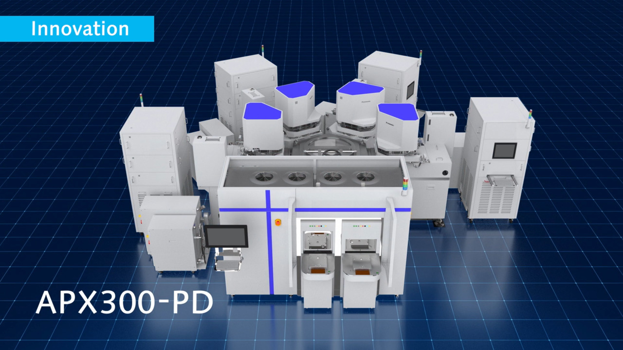
Product lineup
| Model |
APX300-DM |
APX300-PD |
|---|---|---|
| Exterior | Single chamber configuration supports a wide range of applications from R & D to mass production |
Multi-chamber system with up to 4 chambers (Class 10 compatible), ideal for mass production lines |
| Features |
※Applicable range may vary depending on processing conditions and material characteristics. |
|
| Target wafer |
Dicing example
Plasma dicing of plastic materials like DAF
▲Process case study
Plasma dicing of laminated wafer such as insulated film and WoW structure
Various other case studies of dicing
Related products
Plasma Dicer
APX300-DM
Reduces damages, takes more chips and increases productivity with the next generation plasma dicing technology.
Plasma Dicer
APX300-PD
Multi-chamber system (up to four chambers) contributes to automation and high productivity in semiconductor factories